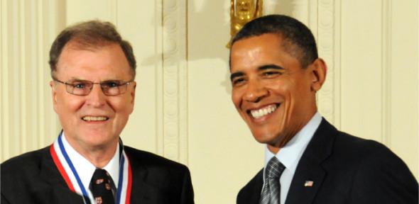
The Cambridge Engineering alumnus who designed and built the first-ever digital camera stood side by side with Barack Obama at The White House as he was honoured with a lifetime achievement award.
Dr Michael Tompsett was handed a National Medal of Technology and Innovation, the highest honour given by the United States government to engineers and inventors. Dr Tompsett has also received two other lifetime awards; the New Jersey Inventors Hall of Fame 2010 Pioneer Award, and the 2012 IEEE Edison Medal. The thermal-imaging camera tube developed from his invention also earned a Queen's Award in 1987.
Dr Tompsett is a British-born physicist and former researcher at English Electric Valve Company (EEV now E2V) in Chelmsford, who later moved to Bell Labs in America. He is best known as the developer of Charge-Coupled Device (CCD) imagers used in digital cameras.. This and his other achievements led to several enabling technologies.
As a PhD student and associate here at the Department of Engineering from 1962 to 1966 Dr Tompsett built a Reflection High Energy Electron Diffraction (RHEED) system to study surfaces. While at E2V, he built the first ultra-high-vacuum RHEED system with in-situ deposition to study the structures of thin-films of lead oxide as they were deposited. This understanding was needed to make Plumbicon television camera-tubes. He consulted with VacGen (now VG Scienta) to make a commercial system, the first of which was sold to IBM Labs.
In 1968 while still at EEV, Dr Tompsett invented the un-cooled Pyro-electric thermal-imaging camera tube. He also invented a solid-state version, which is now the basis for thermal imagers made today. These imagers are used with great impact by the military for night-vision, by firefighters to see through smoke, and for other search-and-rescue and civilian uses worldwide.
In 1969, he moved to New Jersey, USA with his wife, and joined AT&T Bell Telephone Laboratories, where he made the first CCD, and led the development of CCDs. His group developed CCD linear and television imagers, and was the first to demonstrate an all solid-state color camera.
In 1979, he pioneered the development of the first, integrated-circuit, data modem using Metal Oxide Semiconductor (MOS) silicon switched-capacitor filters and a patented Automatic Gain Control circuit. This was the first mixed analog-digital integrated circuit/system to go into manufacture. This technology has now grown into a multi-billion dollar industry.
In the 1980s Dr Tompsett applied himself to finding a solution to a major challenge to reduce the size, power and cost of digitizing video signals from imagers and scanners. He invented an integrated, two-step recycling video analog-digital converter. These are now in mass production. After a 6 year job running an Electron Device Laboratory for the US Army, he started his own company. We are pleased to see one of our alumni, being awarded for his many groundbreaking innovations.
Below Dr Tompsett reflects on his working life on the cutting edge in Britain and in the USA.
Despite reading Physics as an undergraduate at Cambridge, it was an easy transition to the Department of Engineering for a Ph.D. My father was an engineer and I had never thought of doing anything else. I had already worked 2 gap years as an engineer apprentice prior to going to Cambridge. Using a modified idea from my supervisor, I built an electron-beam vacuum system and used it to study the physical structure of materials. When I joined the EEV Company (now E2V), they were facing a severe material problem trying to deposit lead-oxide for a new type of camera tube. I built an ultra-high-vacuum version of my Cambridge instrument and successfully studied these films as they were grown. Little did I know how ubiquitous this technology would become. In 1969, I consulted for Vacuum Generators Ltd (now VG Scienta), who built a system for a researcher at IBM, who was trying to grow epitaxial III-V films for high speed transistors. Today these films are made by the acre for laser and light-emitting diodes and still monitored in the same way.
In 1968, while still at EEV, I invented two uncooled thermal-imaging technologies. One was a pyro-electric camera tube. The resulting cameras are hand-held, can see in the dark and through smoke using infrared light to sense minute changes in temperature. They are deployed with the military and civilian search-and-rescue services. One quote describes these cameras as "The most fantastic piece of rescue equipment I've seen in 29 years as a career firefighter. It has revolutionised firefighting and rescue …You see through the room as though the smoke wasn't there." The other invention was an integrated-circuit version of an uncooled thermal imager, which had to wait 25 years for the technology to become available, but today such imagers are much smaller, use less power and have higher performance. I had the pleasure of being asked to write 2 chapters in a book on uncooled imaging 25 years later.
I joined Bell Laboratories in 1969 with the goal of developing solid-state cameras. Shortly after, Boyle and Smith, also at Bell Labs, came up with the CCD concept as applied to serial memory, but they had no insight into its application to imaging, and took no part in the invention, or subsequent development of CCDs or CCD imagers. This led to a later controversy, since the first patent for CCD Imagers is in my name. The Nobel Committee overlooked this patent, and awarded Boyle and Smith the 2009 Nobel Prize for Physics using the citation: "for the invention of an imaging semiconductor circuit - the CCD sensor", which actually reads on my patent. I made the first CCD in 1970, and developed the first CCD imagers and cameras, which we demonstrated to the world. The first discrete-pixel CCD color image, a picture of my wife, was featured on the cover of Electronics Magazine in January 1973. One of the structures in my original patent is still the basis for the design of imagers in space exploration (Mars Voyager) and astronomy. I wrote a book with one of my colleagues on CCDs Charge Transfer Devices that was translated into Japanese and Russian, which was also a source of great satisfaction.
In 1979 I transferred my attention to another area. I set out to reduce the size, power and cost of a then new piece of equipment, a 2400bps (!!) data modem. I was aware of some ideas on MOS analog circuit components, but no one had attempted to integrate all these into a viable mixed analog-digital integrated circuit. Anticipating the compelling advantages in power, size and cost, I initiated a development which almost foundered on the fact that the dynamic range required was much higher than the circuits were capable of. I invented a solution to that problem, and the resulting chip met the specs and became the first MOS mixed analog-digital integrated-circuit chip to go into manufacture anywhere. Such ICs have now become ubiquitous. I continued working in this area on the development of telecom chips, including the low-frequency/high-frequency analog-digital interface chip for the first GSM mobile phone for Nokia.
Over several years I had tried to solve the problem of making an integrated-circuit high performance video analog-to-digital converter I finally succeeded with a 2 step recycling structure, that was brilliantly implemented by a colleague, and led to the very first viable silicon integrated 10-bit video digitization chip in 1989. In the first year of manufacture this generated $25M revenue and is now found in scanners, cameras, mobile phones etc. This is the unseen circuit that provides the input to the sophisticated digital-signal-processing of today's digital photography. Paradoxically this is what also enables MOS imagers to now successfully compete with CCDs, although MOS sensors were actually suggested by Peter Noble of Plessey in 1967.
I took an early retirement option from Bell Labs in 1989 and turned to inventing my own job. I had an idea to have software developed to do optimised routing similar to that used to layout integrated circuits. This would be used to read US Geological Survey digital maps, and provide audible directions for, say, people doing deliveries. The area was wide open then, but much to my future chagrin, I dropped the idea to become the Director of Electron Device Research for the US Army for 6 years.
Having worked for the 2 largest organisations, AT&T and the US Government, I decided to work for the smallest, my own. My wife is a psychiatrist and provided impetus for me to develop an Electronic Medical Records and Practice Management software, which my company now sells for healthcare offices nationwide.
I am proud and lucky enough to be recognised with 3 lifetime awards for having blazed several new trails for technologies that continue to be used today. However all inventions are a product of their time and the ideas of many people. I have been lucky to be in situations where I was able to synthesize some of those ideas. I should also point out that I have always had talented people working with me, who made major contributions. A very important aspect for developing new ideas, particularly in today's always-on environment, is to take time out to look around and define a tangible problem to be solved, since inside every large problem there is always a little problem waiting to be solved. The latin motto of my High School was "Incipe", "Begin", which I must have taken to heart. I would encourage all aspiring engineers to "Begin" repeatedly and be willing to deliberately move out of their comfort zone into new areas. I have to give credit to Brentwood School, and the University of Cambridge Departments of Physics and Engineering for teaching me these things, and all the smart people that I have worked with over the years for their stimulation.
