No one disputes that carbon nanotubes have the potential to be a wonder technology: their properties include a thermal conductivity higher than diamond, greater mechanical strength than steel – orders of magnitude by weight – and better electrical conductivity than copper.
Since 2006, worldwide carbon nanotube production capacity has increased at least tenfold.
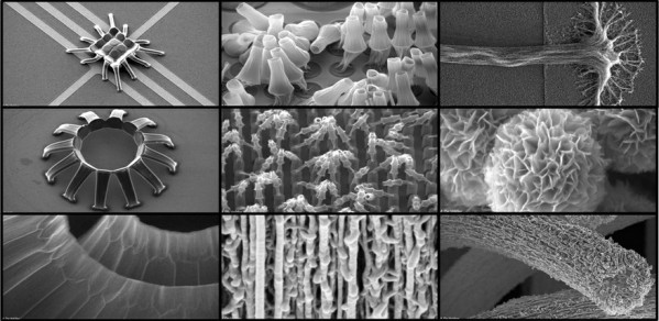
Dr Michael De Volder
But, like other 'great technologies of the the future', are we over hyping nanotubes? Are they near passing the real test – that of widespread practical use? The answer is a qualified yes. The success of carbon nanotubes (CNTs) is proved by a surprising statistic: worldwide commercial production capacity presently exceeds several thousand tons per year, according to Dr Michael De Volder, recently appointed lecturer at the Department of Engineering's Institute for Manufacturing. But it's a level of production that has taken around 20 years to achieve.
"The beginning of widespread carbon nanotube research was preceded in the 1990s by the first scientific report of CNTs, although hollow carbon nanofilaments were reported as early as the 1950s," Dr De Volder says. "However, carbon nanotube related commercial activity has grown most substantially during the past decade. Since 2006, worldwide carbon nanotube production capacity has increased at least tenfold."
Dr De Volder’s recent science review paper of commercially available carbon nanotube applications gives a flavour of just how widespread a real impact the technology is starting to make [M. De Volder et al, Science 339, 2013]. Take water purifiers, for example, the size, surface area and adsorption properties of carbon nanotubes make them an ideal membrane for filtering toxic chemicals, dissolved salts and biological contaminants from water. US company Seldon Technologies has developed the MineralWater System using its “Nanomesh Purification Technology” – a carbon nanotube filtration system – to do just that. The company says its system delivers drinking water without the use of chemicals, heat, or power: vital for use in developing countries where it is most needed. The filter removes pathogens and contaminants such as viruses, bacteria, cysts and spores, delivering water that meets or exceeds the USEPA Drinking Water Standard. It is suitable for use in homes, offices, schools, clinics, and other commercial environments, Seldon says.
The huge surface area of carbon nanotubes is also being exploited when they are used as the electrodes in batteries and capacitors to provide more current and better electrical and mechanical stability than other materials. Worldwide research efforts in this field have fostered the development of commercial activities in companies such as Showa Denko (Batteries, Japan), and FastCAP (Supercaps, US). The properties of carbon nanotubes make them ideal for enhancing different kinds of structures – for example, sports equipment, body armour, vehicles, etc., where they are being widely used. The nanotubes create networks within the composite material for instance to increase stiffness and material damping.
Sports manufacturers use them in tennis and badminton rackets, and bicycle frames. But while carbon nanotubes are being used in practical applications, it doesn't imply their more widespread use will not be problem free.
"There are a number of obstacles which we haven't solved yet," Dr De Volder says. "Particularly in high end targets, like the search for better transistors, the exact morphology of the nanotube and the orientation of the graphene lattice with respect to the tube axis – referred to as its chirality – is really important. At this moment, we have little ability to synthesise carbon nanotubes with specific types of chirality and it is this that determines the semiconducting versus conducting properties of the carbon nanotubes.
"One of the interesting things happening is the improvement in computer simulations of how carbon nanotubes are synthesised, which will hopefully enable us to tweak the fabrication process. And electron microscopy is making it possible to look at the carbon nanotubes while they are being formed, which is helping improved understanding of the process."
Dr De Volder himself is working on the challenge of mass producing devices featuring hundreds to thousands of nanotubes.
"Unfortunately, when you bring them together in large numbers, the figures of merit for their properties are often disappointing compared with what you get from an individual carbon nanotube. I am trying to develop techniques for bringing particles together in more efficient ways, or looking at new emerging properties of the materials depending on how you bring the carbon nanotubes together."
Nevertheless, progress is now happening with SWNTs, with UK company Thomas Swan being a world leader in making SWNTs with its Elicarb material, now being used in areas like advanced composites, electronics, energy storage, print, paper and packaging and fuel cells.
Another recent development in SWNTs – announced in June by Linde Electronics – is the development of a carbon nanotube ink for use in displays, sensors and other electronic devices. Potential applications include smartphones with a roll up screen and a see through GPS device embedded in the windshield of a car.
"Linde is now making its nanotube inks available to developers," says Dr Sian Fogden, market and technology development manager for Linde's nanomaterials unit. "These inks contain single walled carbon nanotubes and are produced without damaging or shortening the nanotubes and therefore they preserve the unique nanotube properties."
Linde claims this is a landmark development that drastically improves the performance of transparent conductive thin films made from the inks and opens the door for the development of carbon nanotube applications in not only consumer electronics, but also the healthcare and sensor manufacturing sectors.
Because nanotubes are long and thin, they have high van der Waals forces between them and they stick together. The standard way to separate them is by using high powered sound waves. But this can damage the nanotubes and affect their properties.
"With our inks, we use a process called Salt Enhanced Electrostatic Repulsion (SEER) that doesn't require sonication but which produces solutions of individual carbon nanotubes while maintaining the length of the nanotube," Dr Fogden says. "Only very recently have products such as touch screens begun to be produced which contain single walled carbon nanotubes and these devices have yet to be launched into the full consumer market. Only when the raw carbon nanotube material can be fully processed in a reliable and repeatable manner will they be used in consumer electronics on a large scale."
Another recent intriguing development in electronics and computing comes from US company Nantero, which says it is commercialising carbon nanotube based semiconductor devices, including memory, logic and others.
"We have developed NRAM, a high density nonvolatile RAM and the aim is for it to serve as a universal memory technology," says ceo Greg Schmergel. "NRAM can be manufactured for both standalone and embedded memory applications and samples have already been shipped to selected customers and are under development at several production cmos fabs by Nantero and its licensees. These samples are multimegabit arrays that demonstrate high yield, high speeds, reliability and low power consumption."
Nantero claims it is the first company to actively develop semiconductor products using carbon nanotubes suitable for production in a standard cmos fab.
"The main obstacle in the past has been the fact that carbon nanotubes have not been compatible with existing semiconductor fabs," Schmergel says. "At Nantero, we have solved that by developing a cmos compatible carbon nanotube material that can be accepted into any fab in the world and manufacturing processes compatible with existing semiconductor manufacturing equipment. So our memory and other carbon nanotube devices can be made in any cmos fab at high volumes.
Using existing processes means reliability and reproducibility is far higher." Nantero's microelectronic grade carbon nanotube material is now available commercially through licensee Brewer Science.
This could be a pointer to the longer term future, involving mainstream computing. At Stanford University recently, a team announced the first functioning computer built from carbon nanotubes. Despite featuring just 178 transistors and running at 1kHz, the computer is nevertheless 'Turing complete', meaning it can do anything today's machines can do, just much slower.
But, in a few years time, billions of carbon nanotubes may be on our desks and in our pockets.
http://www.nanomanufacturing.eng.cam.ac.uk/
