Department of Engineering researchers as part of an international collaboration have developed a new method for growing ‘hybrid’ crystals at the nanoscale, in which quantum dots – essentially nanoscale semiconductors – of different materials can be sequentially incorporated into a host nanowire with perfect junctions between the components.
The key to building functional nanoscale devices is to control materials and their interfaces at the atomic level.
Dr Stephan Hofmann
A new approach to self-assemble and tailor complex structures at the nanoscale, developed by an international collaboration led by the University of Cambridge and IBM, opens opportunities to tailor properties and functionalities of materials for a wide range of semiconductor device applications.
The researchers have developed a method for growing combinations of different materials in a needle-shaped crystal called a nanowire. Nanowires are small structures, only a few billionths of a metre in diameter. Semiconductors can be grown into nanowires, and the result is a useful building block for electrical, optical, and energy harvesting devices. The researchers have found out how to grow smaller crystals within the nanowire, forming a structure like a crystal rod with an embedded array of gems. Details of the new method are published in the journal Nature Materials.
“The key to building functional nanoscale devices is to control materials and their interfaces at the atomic level,” said Dr Stephan Hofmann of the Solid State Electronics and Nanoscale Science Group, one of the paper’s senior authors. “We’ve developed a method of engineering inclusions of different materials so that we can make complex structures in a very precise way.”
Nanowires are often grown through a process called Vapour-Liquid-Solid (VLS) synthesis, where a tiny catalytic droplet is used to seed and feed the nanowire, so that it self-assembles one atomic layer at a time. VLS allows a high degree of control over the resulting nanowire: composition, diameter, growth direction, branching, kinking and crystal structure can be controlled by tuning the self-assembly conditions. As nanowires become better controlled, new applications become possible.
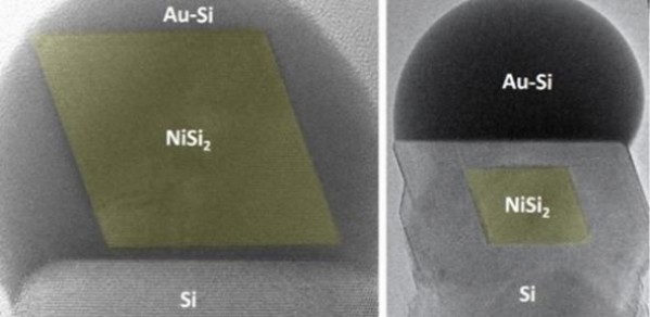
The technique that Stephan and his colleagues from the Department, including Dr Federico Panciera, and IBM developed can be thought of as an expansion of the concept that underlies conventional VLS growth. The researchers use the catalytic droplet not only to grow the nanowire, but also to form new materials within it. These tiny crystals form in the liquid, but later attach to the nanowire and then become embedded as the nanowire is grown further. This catalyst mediated docking process can ‘self-optimise’ to create highly perfect interfaces for the embedded crystals.
To unravel the complexities of this process, the research team used two customised electron microscopes, one at IBM’s TJ Watson Research Center and a second at Brookhaven National Laboratory. This allowed them to record high-speed movies of the nanowire growth as it happens atom-by-atom. The researchers found that using the catalyst as a ‘mixing bowl’, with the order and amount of each ingredient programmed into a desired recipe, resulted in complex structures consisting of nanowires with embedded nanoscale crystals, or quantum dots, of controlled size and position.
“The technique allows two different materials to be incorporated into the same nanowire, even if the lattice structures of the two crystals don’t perfectly match,” Stephan said. “It’s a flexible platform that can be used for different technologies.”
Possible applications for this technique range from atomically perfect buried interconnects to single-electron transistors, high-density memories, light emission, semiconductor lasers, and tunnel diodes, along with the capability to engineer three-dimensional device structures.
“This process has enabled us to understand the behaviour of nanoscale materials in unprecedented detail, and that knowledge can now be applied to other processes,” Stephan said.
The original version of this article appeared on the University of Cambridge website.
