Researchers from the Department of Engineering have designed a new type of pixel element which could make three-dimensional holographic displays possible.
A large amount of surface area is being underutilised, which could be used to store information
Calum Williams
Real-time dynamic holographic displays, long the realm of science fiction, could be one step closer to reality, after researchers from the Department developed a new type of pixel element that enables far greater control over displays at the level of individual pixels. The results are published in the journal Physica Status Solidi.
As opposed to a photograph, a hologram is created when light bounces off a sheet of material with grooves in just the right places to project an image away from the surface. When looking at a hologram from within this artificially-generated light field, the viewer gets the same visual impression as if the object was directly in front of them.
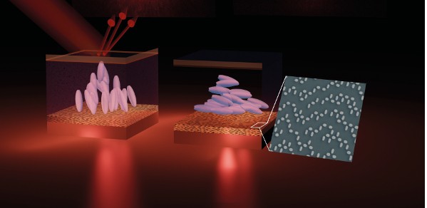
Currently, the development of holographic displays is limited by technology that can allow control of all the properties of light at the level of individual pixels. A hologram encodes a large amount of optical information, and a dynamic representation of a holographic image requires vast amounts of information to be modulated on a display device.
A relatively large area exists in which additional functionality can be added through the patterning of nanostructures (optical antennas) to increase the capacity of pixels in order to make them suitable for holographic displays.
“In a typical liquid crystal on silicon display, the pixels’ electronics, or backplane, provides little optical functionality other than reflecting light,” said Calum Williams, a PhD student in the Photonics Group and the paper’s lead author. “This means that a large amount of surface area is being underutilised, which could be used to store information.”
Calum and his colleagues have achieved a much greater level of control over holograms through plasmonics: the study of how light interacts with metals on the nanoscale, which allows the researchers to go beyond the capability of conventional optical technologies.
Normally, devices which use plasmonic optical antennas are passive, meaning that their optical properties cannot be switched post-fabrication, which is essential for real-world applications.
Through integration with liquid crystals, in the form of typical pixel architecture, the researchers were able to actively switch which hologram is excited and there which output image is selected.
“Optical nanoantenas produce a strong interaction with light according to their geometry. Furthermore, it is possible to modulate this interaction with the aid of liquid crystals,” said co-author Yunuen Montelongo, a PhD student in the Photonics Group.
The work highlights the opportunity for utilising the plasmonic properties of optical antennas to enable multi-functional pixel elements for next generation holographic display technologies.
Scaling up these pixels would mean a display would have the ability to encode switchable amplitude, wavelength and polarisation information, a stark contrast to conventional pixel technology.
This article was originally published on the University of Cambridge website.
