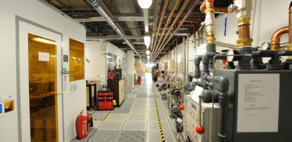

The University of Cambridge Electrical Engineering Division building opened in 2006 and houses custom-built state-of-the-art photonics and electronics research and prototype development facilities across approx. 5,000m2 of lab space, including class 100 (140 m2), class 1000 (140 m2) and class 10k (160 m2) clean room facilities.
The Engineering Clean Facility is available to be used by academic and industry users. If you are interested in accessing the Facility, please contact Dr Andrew Flewitt, who will be able to provide up to date information regarding access charges and training.
Available equipment includes:
Specialist deposition systems:
- Cold- and hot-walled, thermal and plasma enhanced CVD reactors for the growth of graphene and carbon nanotubes (9 different reactors ranging from high vacuum to atmospheric pressure)
- Cold- and hot-walled CVD reactors for the growth of semiconducting nanowires
- ECWR plasma and Filtered Cathodic Arc deposition systems for the deposition of amorphous carbon films
- Thermal and plasma enhanced CVD reactors for the deposition of amorphous Si thin films
- Plasma enhanced and thermal Atomic Layer Deposition (ALD) reactors
- Remote plasma and ion beam sputterer for the deposition of functional oxide thin films
- Thermal and e-beam evaporators
- Magnetron, RF and DC sputterers
- Plasmaquest HiTUS sputter system
Device processing facilities:
- Optical Mask Aligners
- (0.5µm with 2µm front-to-backside alignment)
- E-beam Lithography
- Reactive Ion etching (RIE and DRIE) systems
- Acid and Solvent Bays
- Annealing and oxidation furnaces
- Wire and Device bonders
- Inkjet Printer
- Ultra-centrifuges and Sonicators
- Langmuir-Blodgett equipment
Characterisation and testing facilities:
- Surface and optical profilometers
- UV-Vis and FTIR spectrometers
- Raman spectroscopy and PL systems
- Ellipsometry systems
- A range of Electrical Probe stations
- We have a semi-automatic probe station, temperature stages up to 200°C and can do both DC and high frequency measurements up to 3GHz
- Bruker Dimension Icon Atomic Force (AFM), Optical and Electron (FEI High resolution SEM, TEM shared with Physical Sciences) Microscopes
- Agilent PNA microwave test engine.