Dr Felice Torrisi, University Lecturer in Graphene Technology, has been awarded a Young International Researchers' Fellowship from the National Science Foundation of China to look at how graphene and two-dimensional materials could enable printed and flexible eyes.
It might eventually be possible to embed these printed, flexible optoelectronic devices into clothes, packaging, wall papers, posters, touch screens or even buildings
Dr Felice Torrisi
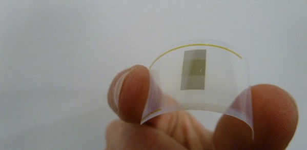
The vision is to create a technology for cheap flexible cameras that can be printed or stamped on plastic or paper. "For example it might eventually be possible to embed these printed, flexible optoelectronic devices into clothes, packaging, wall papers, posters, touch screens or even buildings. Everybody with a printer at home will be able to print their own "artificial eye" and physically stick it to a flexible mobile phone" Felice said.
The goal of the 18 month project is to design, develop and characterize inkjet printed 2D crystal-based flexible photodetectors and study their integration with commercial electronics.
“Photodetectors are needed in cameras, automotive applications, sensing and telecommunications, medical devices and security” he says. “If these could be made flexible they could be integrated in clothes, rolled up or printed over any irregular surface substantially increasing the quality of printed and flexible electronics.”
The current generation of flexible photoactive materials, based on organic polymers have a slow response time (few milliseconds), which is too slow for photodetection. This represents a strong limitation for flexible electronics in a wide range of applications, from active matrix displays to ultrafast light detectors and gas sensors. Moreover organic polymers suffer from chemical instability at room conditions (temperature and pressure), thus requiring extra protective layers or special handling of the printed devices, leading to an increase in cost.
Graphene, the ultimate thin membrane along with a wide range of two-dimensional (2D)-crystals (e.g. hexagonal Boron Nitride (h-BN), Molybdenum Disulfide (MoS2) and Tungsten Disulfide (WS2)), have radically changed the landscape of science and technology with attractive physical properties for (opto)electronics, sensing, catalysis and energy storage. These 2D crystals can be exfoliated from layered compounds. The layered compounds can be conductive, semiconducting or insulating and their electronic properties depend on the number of layers. For example, graphene is highly conductive, flexible and transparent and it is superior to conductive polymers in terms of cost, stability and performance; whereas MoS2 is optically active once reduced to a single 2D layer, with a fast response time and excellent environmental stability.
In 2012 Drs Felice Torrisi, Tawfique Hasan and Professor Andrea Ferrari at the Cambridge Graphene Centre invented a graphene ink which conducts electricity and can be printed by a standard inkjet printer. The graphene-based ink enables cost-effective, printed electronics on plastic.
Felice explains: “Other conductive inks are made from precious metals such as silver, which makes them very expensive to produce and process, whereas graphene is both cheap, environmentally stable, and does not require much processing after printing”.
“We used a simple sonication and centrifugation process to unveil graphene potential in inks and coating for printed electronics”
Over the last two years Dr Torrisi and the team at the Cambridge Graphene Centre have been looking to formulate a set of inks based on various 2D crystals, setting a new platform for printed electronics. Felice says: “This will create an entirely new set of tools for printable electronics with conductive, semiconducting and insulating properties, with a faster response time, outperforming the current organic semiconducting inks, enabling printed, flexible photodetectors and possibly paving the way for printed flexible photo-cameras”.
“When light impinges on a semiconducting 2D crystal (e.g. MoS2), due to their 2D nature, electrons and holes are generated with a higher efficiency than the current photodetectors based on silicon”
The project, funded by the National Natural Science Foundation of China, looks into how to design printed flexible photodetectors based on graphene and 2D crystal-inks.
“The optical response of the printed 2D crystal inks, combined with their flexibility on plastic substrate and environmental compatibility, are key benefits to improving flexible optoelectronics”
